What Is A P-Type Semiconductor?
A p-type semiconductor is a type of semiconductor material that shows increased conductivity when donor impurities are introduced. These donor atoms are typically elements from Group III of the periodic table, like boron (B), aluminium (Al), or gallium (Ga), and have three valence electrons in their outer shell.
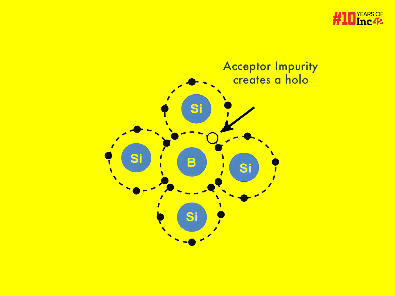
These elements are called acceptor impurities because they create holes, which are vacancies for electrons. When introduced into the crystal lattice of a Group IV semiconductor like silicon (Si) or germanium (Ge), which possess four valence electrons, the acceptor atom’s three valence electrons form covalent bonds with three neighbouring semiconductor electrons.
However, one electron remains absent from the bond. This space is called a ‘hole’. When an electric field is applied, the electrons from neighbouring semiconductor atoms move into the space and a ‘hole’ current is generated, which can be perceived as a positive charge movement. This ‘hole’ population in the conduction band contributes to the overall conductivity of the p-type semiconductor.
How Is A P-Type Semiconductor Created?
A p-type semiconductor is created through doping, where a carefully controlled amount of impurity atoms are introduced into a pure semiconductor crystal. The following is a general breakdown of the steps involved:
- Starting Material: The process begins with a pure semiconductor, typically silicon (Si) or germanium (Ge). These elements have four valence electrons in their outer shell, allowing them to form a stable crystal structure with covalent bonds. However, in their pure state, they have very low conductivity.
- Doping With Acceptor Atoms: Elements from group III of the periodic table, such as boron (B), aluminium (Al), or gallium (Ga), are used as the dopant. These elements have three valence electrons, one less than a pure semiconductor.
- Integration Into Crystal Lattice: During manufacturing, a tiny amount of the acceptor element is introduced into molten silicon or germanium. As the material cools and solidifies, the donor atoms become integrated into the semiconductor crystal lattice.
- Creating Holes: When the dopant atoms integrate into the crystal structure, they bond with the surrounding semiconductor atoms using their three valence electrons. However, since they only have three electrons, one bonding spot still needs to be fulfilled. This creates a vacancy for an electron, essentially a ‘hole’ with a positive charge (the absence of a negative electron).
- Increased Conductivity: While there are still some electrons present in the pure semiconductor material, the introduced holes become the majority charge carriers in the doped semiconductor. This means that the holes are more likely to move and conduct electricity when an electric field is applied.
Group III Elements & P-Type Semiconductors
Group III elements play a crucial role in creating n-type semiconductors. Here’s the connection, explained from a more technical perspective:
- Electronic Structure: Elements in Group III of the periodic table possess a specific electronic configuration. Their atoms’ outer shells hold three valence electrons and their valence shell electron configuration is defined as ns² orbital notation (where n is the principal quantum number). This contrasts with Group IV elements like silicon and germanium, which have a notation of electrons ns²np² configuration.
- Doping & Lattice Substitution: A small amount of a Group III element is introduced into the intrinsic silicon or germanium crystal lattice during doping. These dopant atoms substitute a silicon/germanium atom within the lattice structure.
- Donor Impurity Levels: The key aspect lies in the dopant’s electronic structure. Three of the valence electrons from the Group III element participate in covalent bond formation with the four nearest neighbouring silicon/germanium atoms, replicating the bonding scheme of the original lattice.
However, the absence of a fourth valence electron in the Group III element causes a space within the crystal lattice. This creates an acceptor impurity level within the semiconductor bandgap.
- Holes: When a Group III element is used as a dopant in a semiconductor, it can’t form the same number of covalent bonds as the original semiconductor atom. This creates a vacancy for an electron, essentially a ‘hole’ acting like a positive charge carrier.
- N-Type Characterisation: A p-type semiconductor is specifically a semiconductor that has been doped with elements from Group III. The presence of these holes makes them the majority charge carriers in the material. This allows the p-type semiconductor to conduct electricity by the movement of these holes when an electric field is applied.
How Are P-Type Semiconductors Used In Electronics?
P-type semiconductors are fundamental building blocks in a wide range of electronic devices:
- Diodes: A diode is a basic electronic component that allows current to flow in one direction only. P-type semiconductors are combined with n-type semiconductors (doped with Group V elements) to form a p-n junction, the heart of a diode. In this junction, the flow of holes and electrons is restricted, enabling the diode’s rectification properties. P-type semiconductors are thus essential for applications like converting AC to DC, voltage regulation, and signal detection.
- Transistors: Transistors are the workhorses of modern electronics, acting as amplifiers and switches. Bipolar Junction Transistors (BJTs) are a common type that utilises both p-type and n-type regions. The base region of a BJT is typically made from a p-type semiconductor. By controlling the current flow through the base, the BJT can amplify a small input signal into a much larger output signal. This ability to control current makes BJTs vital for electronic circuits such as amplifiers, logic gates, and microprocessors.
- Integrated Circuits (ICs): ICs are tiny electronic circuits containing millions of transistors and other components. These complex circuits are built on a silicon wafer, where p-type and n-type regions are strategically placed to create various functionalities. The precise control over p-type and n-type regions allows engineers to design intricate circuits for computers, smartphones, and countless other electronic devices.
- Other Applications: P-type semiconductors also play a role in various other electronic components, including solar cells, LEDs and photodetectors. Their ability to interact with light and respond to its presence makes them valuable in optoelectronic applications.


